- 您现在的位置:买卖IC网 > Sheet目录114587 > 550BDFREQBG (SILICON LABORATORIES) VCXO, CLOCK, 10 MHz - 945 MHz, LVDS OUTPUT
Si550
2
Rev. 0.5
1. Electrical Specifications
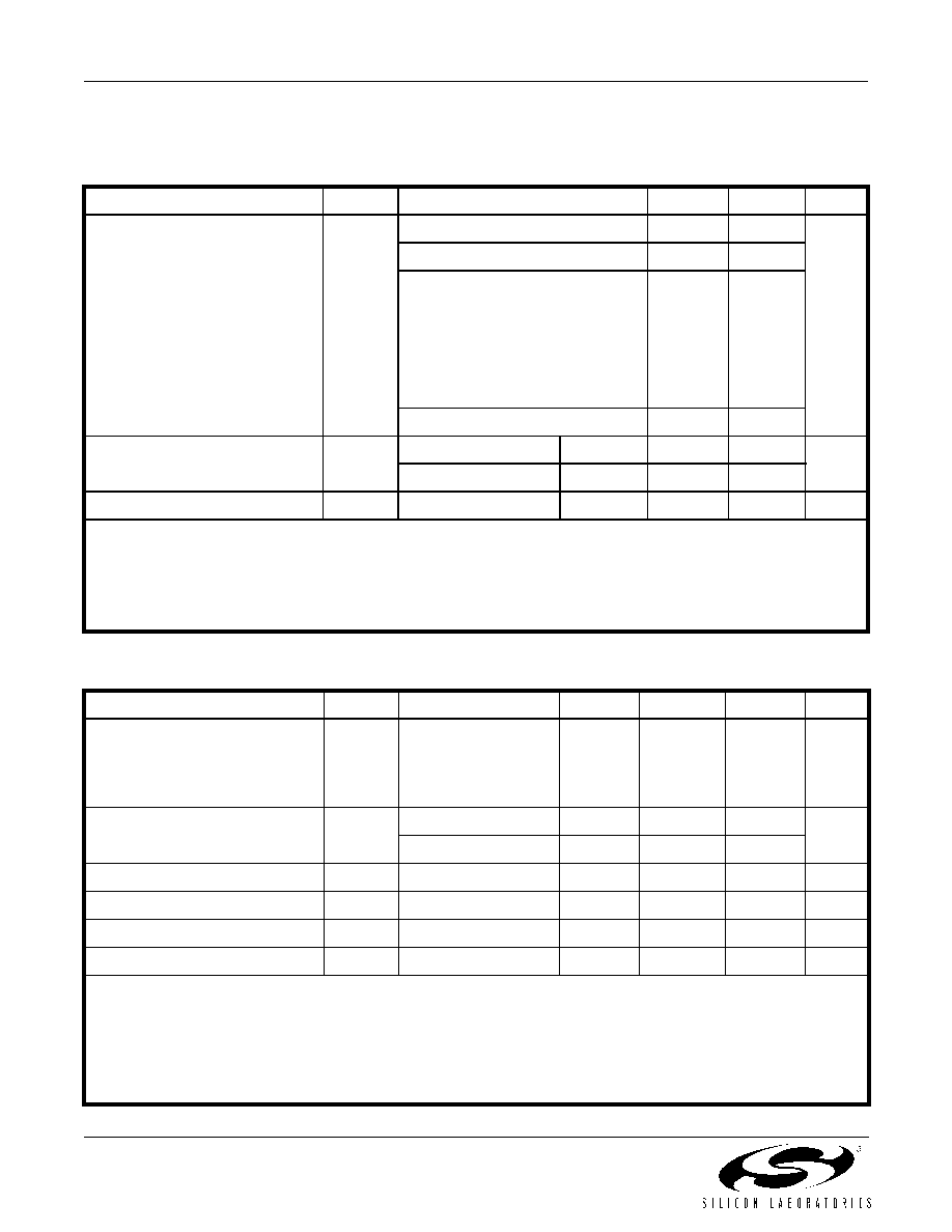
Table 1. Recommended Operating Conditions
Parameter
Symbol
Test Condition
Min
Typ
Max
Units
Supply Voltage1
VDD
3.3 V option
2.97
3.3
3.63
V
2.5 V option
2.25
2.5
2.75
1.8 V option
1.71
1.8
1.89
Supply Current
IDD
Output enabled
LVPECL
CML
LVDS
CMOS
—
120
108
99
90
130
117
108
98
mA
TriState mode
—
60
70
Output Enable (OE)2
VIH
0.75 x VDD
——
V
VIL
——
0.5
Operating Temperature Range3
TA
–40
—
85
C
Notes:
1. Selectable parameter specified by part number. See Section 3. "Ordering Information" on page 7 for further details.
2. OE pin includes a 17 k
pullup resistor to VDD. Pulling OE to ground causes outputs to tristate.
3. If the device is powered up below –20 C and the ambient temperature rises by approximately 105 C during normal
operation, the device will perform a one-time recalibration. The output is squelched for approximately 2–3 ms during
this recalibration.
Table 2. VC Control Voltage Input
Parameter
Symbol
Test Condition
Min
Typ
Max
Units
Control Voltage Tuning Slope1,2,3
KV
10 to 90% of VDD
—45
90
135
180
—
ppm/V
Control Voltage Linearity4
LVC
BSL
–5
±1
+5
%
Incremental
–10
±5
+10
Modulation Bandwidth
BW
9.3
10.0
10.7
kHz
VC Input Impedance
ZVC
500
—
k
Nominal Control Voltage
VCNOM
@ fO
—3/8 x VDD
—V
Control Voltage Tuning Range
VC
0VDD
V
Notes:
1. Positive slope; selectable option by part number. See Section 3. "Ordering Information" on page 7.
2. For best jitter and phase noise performance, always choose the smallest KV that meets the application’s minimum APR
requirements. See “AN266: VCXO Tuning Slope (KV), Stability, and Absolute Pull Range (APR)” for more information.
3. KV variation is ±28% of typical values.
4. BSL determined from deviation from best straight line fit with VC ranging from 10 to 90% of VDD. Incremental slope
determined with VC ranging from 10 to 90% of VDD.
发布紧急采购,3分钟左右您将得到回复。
相关PDF资料
571FKAFREQDGR
VCXO, CLOCK, 10 MHz - 945 MHz, LVDS OUTPUT
571KFAFREQDGR
VCXO, CLOCK, 10 MHz - 945 MHz, CMOS OUTPUT
571MDAFREQDG
VCXO, CLOCK, 10 MHz - 945 MHz, LVPECL OUTPUT
550ME614M400DGR
VCXO, CLOCK, 614.4 MHz, LVPECL OUTPUT
550MH040M000DGR
VCXO, CLOCK, 40 MHz, LVPECL OUTPUT
550MH166M628DGR
VCXO, CLOCK, 166.628 MHz, LVPECL OUTPUT
550ND125M000DGR
VCXO, CLOCK, 125 MHz, LVDS OUTPUT
550CJ153M600DGR
VCXO, CLOCK, 153.6 MHz, CMOS OUTPUT
相关代理商/技术参数
550BE100M000DG
功能描述:VCXO振荡器 SNGL VCXO 6 PIN 7mm x 5mm RoHS:否 制造商:Fox 封装 / 箱体:5 mm x 3.2 mm 频率:19.2 Mhz 频率稳定性:2.5 PPM 输出格式: 封装:Reel 电源电压:3 V 端接类型:SMD/SMT 尺寸:3.2 mm W x 5 mm L x 1.5 mm H 最小工作温度:- 20 C 最大工作温度:+ 75 C
550BE102M400DG
功能描述:VCXO振荡器 SINGLE VCXO 6 PIN 0.5PS RS JTR RoHS:否 制造商:Fox 封装 / 箱体:5 mm x 3.2 mm 频率:19.2 Mhz 频率稳定性:2.5 PPM 输出格式: 封装:Reel 电源电压:3 V 端接类型:SMD/SMT 尺寸:3.2 mm W x 5 mm L x 1.5 mm H 最小工作温度:- 20 C 最大工作温度:+ 75 C
550BE102M400DGR
制造商:Silicon Laboratories Inc 功能描述:OSCILLATOR - Tape and Reel
550BE120M000DG
制造商:Silicon Laboratories Inc 功能描述:
550BE125M000DG
功能描述:VCXO振荡器 SNGL VCXO 6 PIN 7mm x 5mm RoHS:否 制造商:Fox 封装 / 箱体:5 mm x 3.2 mm 频率:19.2 Mhz 频率稳定性:2.5 PPM 输出格式: 封装:Reel 电源电压:3 V 端接类型:SMD/SMT 尺寸:3.2 mm W x 5 mm L x 1.5 mm H 最小工作温度:- 20 C 最大工作温度:+ 75 C
550BE148M500DG
功能描述:VCXO振荡器 SINGLE VCXO 6 PIN 0.5PS RS JTR RoHS:否 制造商:Fox 封装 / 箱体:5 mm x 3.2 mm 频率:19.2 Mhz 频率稳定性:2.5 PPM 输出格式: 封装:Reel 电源电压:3 V 端接类型:SMD/SMT 尺寸:3.2 mm W x 5 mm L x 1.5 mm H 最小工作温度:- 20 C 最大工作温度:+ 75 C
550BE156M250DG
制造商:Silicon Laboratories Inc 功能描述:OSCILLATOR - Trays
550BE156M250DGR
制造商:Silicon Laboratories Inc 功能描述:OSCILLATOR - Tape and Reel